PCB fabrication using old magazine pages
Do you need a PCB?, but tired of going through the torpor of ironing for 45 minutes trying to get that perfect heat transfer. Etching a printed circuit board (PCB) fabrication at home may seem like a daunting task, but with the right tools and techniques, it can be a rewarding and cost-effective endeavor. In this blog, we'll guide you through the intricate steps of crafting your own PCB using a laserjet printer, magazine pages, and a touch of DIY spirit.
Step 1: Printing the Circuit Design
The journey begins with the heart of your PCB—the circuit design. Utilizing a high-quality laserjet printer is crucial at this stage, as better printers yield superior results. Ensure that the print is successful on magazine pages, which will act as the medium for transferring your circuit onto the copper clad surface. If your print is not transferring perfectly to the magazine page, look for a different printer. Newer models work best.
Step 2: Prepping the Copper Clad Surface
The canvas for your PCB masterpiece is the copper clad surface. Thoroughly clean and prep it to guarantee optimal adhesion of the circuit design later on. A clean surface is key to a successful transfer.
Step 3: Alignment of the Print

Precision is the name of the game in PCB fabrication. Align the printed circuit design with the copper clad surface using methods like folding or a trusty glue stick. This ensures that your circuit lands exactly where it needs to be.
Step 4: Acetone Magic


Step 5: The Art of Transfer
Once dry, delicately remove the magazine paper, transferring some of it onto the surface. This thin layer acts as a maskant, protecting the copper during the etching process. For minor transfer mishaps, masking tape can be your saving grace.
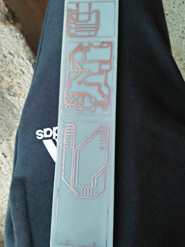
Step 6: Etching Mastery

The moment of truth arrives as you move to the etching phase. Using a mixture of Hydrochloric Acid (HCl) and Hydrogen Peroxide, etch away the exposed copper until your circuit emerges in all its glory. Patience is key here—wait until the process is complete.
Step 7: Rinsing Away Excess
After the etching dance, rinse the PCB with water to remove any remaining acid from the copper clad. This step ensures the longevity and reliability of your DIY creation.
Step 8: Acetone Rinse
A final rinse with acetone washes away the remaining laserjet ink, leaving behind the beautifully etched PCB.

Step 9: Testing the Waters
With your PCB now complete, it's time for the moment of truth. Test and validate the connections using a multimeter in continuity mode. This step ensures that your DIY PCB is not just a work of art but also a functional piece of technology.
Embarking on the journey of DIY PCB fabrication is a testament to the power of creativity and determination. Armed with a laserjet printer, magazine pages, and a handful of chemicals, you can transform your circuit dreams into reality. So, roll up your sleeves, embrace the intricacies of each step, and let the art of PCB fabrication unfold in your hands. Happy crafting!
For this exercise, I thank Lael who made me aware of the technique and my project partner Mercy, for being a really helpful assistant through the process.

Comments
Post a Comment