Are you tired of having to use a bread board for your projects? Do you get tired of all the wires that you use and the hustle of remembering which wire goes to which hole on the bread board😕? Well look no further, you are in the right place😌. This is a simple guide to being able to design and fabricate your own PCB at home for either a personal project of a school project. At the Nakuja project we design our PCB's for avionics and flight control systems using design software such as EasyEDA, print the designs, etch the PCB and do our own soldering of the components onto the PCB.
This blog is designed to give you a step by step guide of the etching process. I hope you enjoy making your PCB!!
Materials required
- Board design (after using EasyEDA, Eagle, etc. to design it)
- clothes iron
- copper clad board
- sand paper
- cupric chloride
- water
- plastic dish or basin
- PCB drill
- soldering iron
- solder wire
NOTE: the etching solution is CORROSIVE and toxic
hence should be handled with care and proper safety clothing (gloves) and in a
space with proper ventilation.
HAZARD SUMMARY
1. Cupric chloride can affect you when breathed in. It can irritate the nose, throat and lungs causing coughing and wheezing.
2. Contact can severely irritate and burn the skin and eyes with possible eye damage.
3. Cupric chloride can irritate the stomach causing salivation, nausea, vomiting, stomach pain and diarrhea.
4. May cause damage to liver and kidneys.
5. Cupric chloride is a DOT CORROSIVE CHEMICAL.
Step one: Design
1. Design the board (single layer)
using various services such as eagle, fritzing or EasyEDA. In this case we used
EasyEDA.
NOTE: to ensure your design is easy to etch and the
tracks appear after etching, some design rules can be set; track width of 1.5, clearance of 0.5. some
tracks such as those supplying 12V should be thicker than the others.
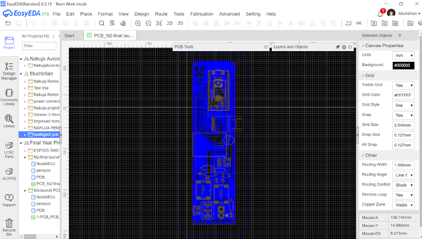 |
Fig 1. PCB design on EasyEDA
|
2. Once the design is done, save your work, then select file, export, pdf as shown below.
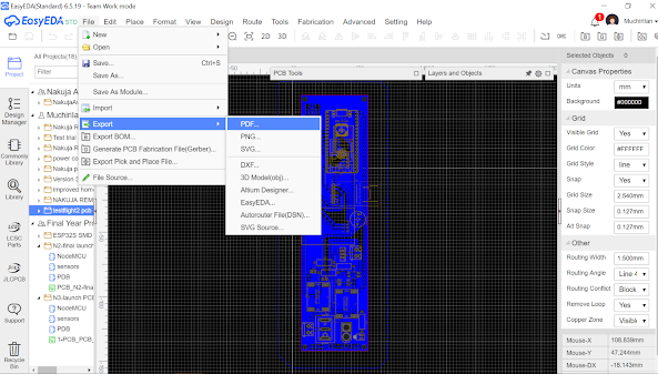 |
| fig 2. Design export step |
3. Select the specific boxes as shown in the diagram below.
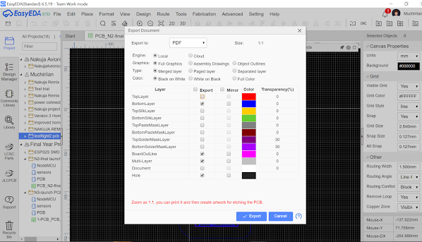 |
| fig 3. Design export properties |
4. Once you are done the downloaded pdf should look like the image shown below.
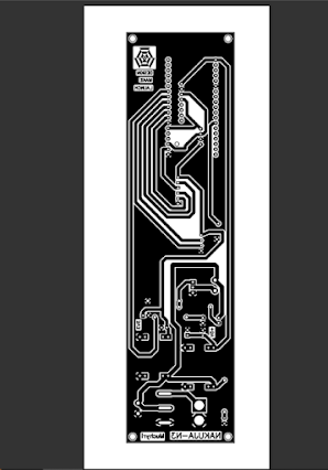 |
| fig 4. Downloaded PDF of the PCB design |
Step two: Print out the design onto the shiny side of a glossy paper
Once you have the pdf as shown above, print out
the design on the shiny side of a glossy paper. When printing some
things are crucial to ensuring the success of the whole process.
1. The printer needs to be a laser printer not
an ink jet.
2. The print dimensions should be actual size not fit.
Step three: Cleaning the copper clad
It is IMPORTANT
for one to wear gloves from this step to handle
the copper clad and etching solution, this helps in avoiding getting oils on
the copper and chemicals and copper filings on your hands.
We clean the copper clad using a fine sand paper. Scrub the surface until it is
bright metallic looking. Wash off the surface with running water to remove the
small copper filings from the sanding.
Step four: Toner transfer
1. Cut out the design leaving some
margins around it.
2. Place the cut out with the glossy
side facing down on the clopper clad.
3. Place the hot clothes iron on top of
the paper and press down for about a minute.
4. Round the clothes iron on the paper
for about 3-5 minutes while still applying pressure on the iron. Do not lift
the paper when hot as this will result in no toner transfer.
5. Place the PCB in water until it
cools and remove the paper using your thumb and fingers. The paper will be
removed and the toner can be easily seen on the copper clad PCB. Ensure that all the paper is removed especially in
between tracks as this might result in the area not getting etched.
 |
| fig 5. PCB placed in water to cool before removing paper |
Step
five: dissolving the copper
1. Dissolve a sufficient amount of
cupric chloride in water.
2. Place the PCB into the solution and
agitate until all the copper around the design has dissolved.
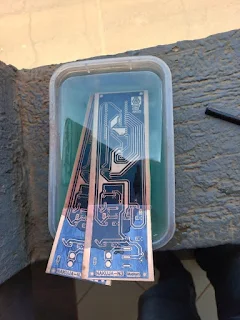 |
| fig 6. Removal of copper |
NOTE: Incase the process is taking long, one can speed up the process by dissolving some more cupric chloride into the solution.
3. Once all the copper is etched, remove the PCB from the solution and rinse it with some soap and water.
4. Scrub off the ink transferred onto the PCB with a kitchen scrubber and soap or rubbing alcohol.
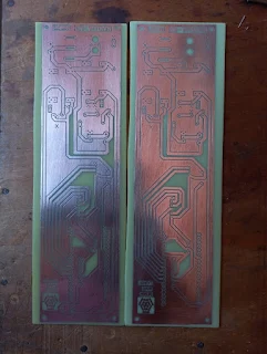 |
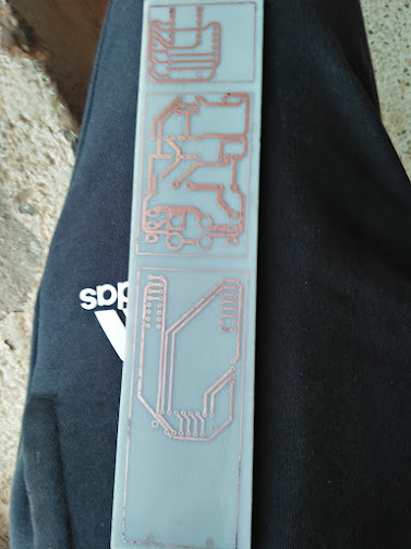
| fig 7. Etched PCBs |
DISPOSAL NOTE: The etching solution eats copper and is somewhat toxic, hence should be disposed with care. Do not pour down the drain if your drain system has copper pipes as it will eat up the copper pipes!
Step six: Drilling of holes
Drill some holes onto the PCB using the PCB drill. Ensure that the drill bit you are using corresponds to the hole size of the hole you are drilling. If it is bigger, it might remove the copper pad thus eliminating an area for soldering.
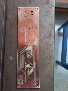 |
| fig 8. PCB with holes of various sizes drilled |
Step 7: Soldering
After completing the PCB drilling, solder the components onto the PCB and this should finalize your PCB.
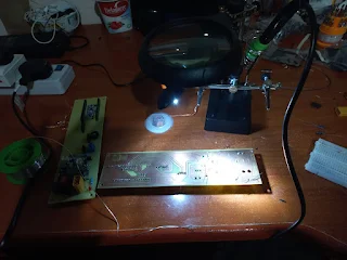 |
fig 9. Soldering process
|
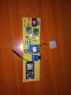 |
| fig 10. PCB with components soldered |
S


Comments
Post a Comment